precision circuit board laser etching
The minimum linewidth is 6 μ M
Laser precision direct writing (or circuit laser precision direct writing laser direct writing circuit laser etching circuit laser precision circuit etching) processing has the following advantages compared with photoresist etching and so on:
Direct processing and molding, without complex mask manufacturing, coating, photolithography and other processes
No pollution, no consumables, no chemical corrosion
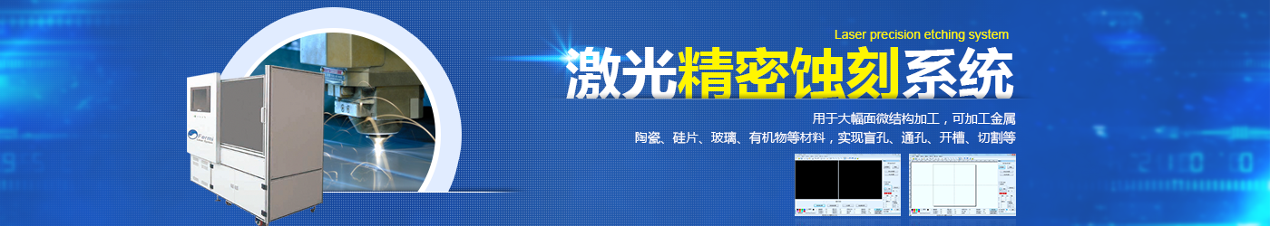
High speed (scanning speed up to 15m / s)
High precision (<± 2 μ m)
There is no material limit, and the base material is glass, ceramics, silicon wafer, organic matter, etc
Minimum processing line width 5 μ M
The processing format can be defined as 300 mm * 300 mm
The laser precision etching direct writing equipment provided by Fermi laser has a minimum processing linewidth of 5 μ m, an overall processing accuracy of ± 2 μ m, a local feature accuracy of less than 2 μ m, and a processing width of 300 * 300 mm. It is used for precision circuit or graphic etching based on glass, sapphire, metal, ceramics, organics, etc.

Fermi laser Copyright © 2016 All Right Reserve沪ICP备15049524号-1